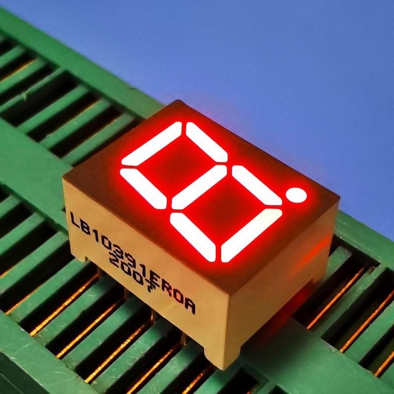
Multiplexed LED Display Power Supply Transient: Decoupling and Rail Droop
This guide treats the multiplexed LED display power supply transient as a power-integrity problem rather than a driver problem: how the scan waveform becomes a current step, where the supply path turns that step into droop, how to place decoupling so the step never leaves the local area, and how to measure the margin that remains.
Quick Answer: The Average Is Not What the Rail Sees
Scanning turns a steady load into a switched one. For one digit period, a single digit conducts at full segment current; the rest are blanked. The supply therefore delivers a pulse train whose peak is set by segment current and the number of segments lit, and whose duty cycle is set by the number of digits and the blanking time. A rail that looks stable on a meter is being asked to supply that peak at the moment each digit turns on.
Whether the rail survives depends on how much charge is stored close to the load and how much impedance sits between that store and the switching elements. Both are layout decisions made long before the first unit is tested.
The Scan Waveform as a Current Step
A scan works by giving each digit a slice of time. Within a slice, the digit's common line is driven and its segment lines are set; between slices, everything is blanked. The current therefore has two edges per slice, and the rise time of each edge is set by the driver's switching speed and by the inductance in the path from the capacitor to the LED.
Three parameters decide how hard the supply is hit. The number of digits sets the duty cycle, because each digit is on for a smaller fraction as the count rises. The segment current sets the peak, because all lit segments in an active digit conduct at once. The blanking time sets the edge rate, because it determines how much of the slice is spent transitioning rather than conducting. The relationship between digit count, segment current and the average the supply must deliver is worked through in the guide to 7 segment display current consumption calculation.
Peak, Average and the Difference That Matters
The arithmetic is simple and the consequences are not. A four-digit display driving one digit at a time has a duty cycle near one quarter, so its average is roughly a quarter of its peak. A supply sized on the average will be asked periodically for four times that value, and the question is whether it can deliver it for the duration of one slice without its output moving.
| Quantity | What sets it | Where it shows up |
|---|---|---|
| Peak current | Segment current multiplied by segments lit in the active digit | Local capacitor discharge, driver ground bounce |
| Average current | Peak multiplied by duty cycle plus quiescent load | Supply sizing, thermal budget, cable rating |
| Step size | Difference between blanked and conducting state | Rail droop, EMI, induced noise on adjacent traces |
| Edge rate | Driver switching speed and path inductance | Radiated emissions, ringing, false triggering |
The step size, not the average, is what the decoupling has to absorb. A quick way to sanity-check a multiplex display peak current figure against a candidate supply is to compare the step with the regulator's specified transient response rather than with its continuous rating.
Supply Path Impedance: Where the Step Becomes Droop
Any current step through an impedance produces a voltage step. The impedance in question is not the regulator's output impedance alone; it is the whole path from the regulator's output capacitor to the LED cathode, including the trace, the connector, the cable and the board's power plane if there is one. At the frequencies involved in a scan, inductance dominates, so a path that measures well with a multimeter can still be a poor conductor for the edge.
Two design decisions shrink that path. Keep the decoupling capacitor's loop to the driver as small as the layout allows, so the high-frequency component never travels to the regulator. And give the return current a path directly under the forward path, so the loop area is small and the inductance with it. Where a display is connected by a cable, the cable's inductance is part of the loop and cannot be decoupled away at the far end; the capacitor has to be on the display side.
Capacitor Placement and Selection
Two capacitors do different jobs and are often specified as one. Most requests for 7 segment decoupling guidance are really asking for both, and the split below is the practical answer: the bulk capacitor holds enough charge that the rail does not sag over a full scan period; the local capacitor supplies the edge. Sizing the bulk part on the average current and the local part on the step is the correct split.
- Local, per driver. Place at the driver's supply pin, with the shortest possible return to its ground pin. This capacitor sees the edge and must have low impedance at the edge's frequency.
- Bulk, per board. Place where the supply enters the display board. This capacitor sees the scan period and its value is set by acceptable sag, not by edge rate.
- ESR and temperature. A capacitor that meets its value at room temperature may lose most of it at the cold end or age out at the hot end; the derating curve matters more than the nominal figure.
- No long stubs. A capacitor connected by a long thin trace is a capacitor in series with an inductor, and at the edge frequency the inductor wins.
For displays built from discrete transistors or from a driver IC, the current path is different and the capacitor placement follows the devices that actually switch; the comparison in BJT vs MOSFET 7 segment display driver is a useful starting point for that decision, and the shift-register architecture changes the pin count and the switching distribution again, as set out in shift register 7 segment display design.
When the Droop Reaches the Driver and the MCU
A rail that dips by a few hundred millivolts at the LED may still be within the driver's operating range and outside the microcontroller's. That asymmetry is why the symptom often appears as a control fault rather than an optical one: the display dims slightly, and the MCU resets or its ADC readings shift at the same time.
Three interactions are worth checking. The driver's own undervoltage behaviour determines whether it blanks cleanly or produces a partial pattern during the dip. The MCU's brown-out threshold relative to the dip depth determines whether a reset is possible. And the analog reference, if it shares the same rail, moves with the droop, which corrupts any measurement the product makes while the display is scanning.
Where the display shares a rail with a supply that has its own compliance requirement, the interaction becomes a headroom question as well; the loss-of-regulation case is described in the guide to LED driver compliance voltage. The radiated side of the same edges is a separate problem, covered in multiplexed LED display EMI.
Measuring Rail Margin on a Scope
The measurement that settles the question is a DC-coupled capture of the rail at the driver's supply pin, triggered on a digit's enable edge, with the time base wide enough to include a full scan period.
- Probe at the driver pin with a short ground lead, not at the connector or the regulator output.
- Trigger on the digit enable signal, not on the supply, so every capture starts at the same point in the scan.
- Record the minimum rail value and the recovery time to the nominal value.
- Repeat with every digit lit, since the worst pattern is rarely the one a test routine produces by default.
- Repeat at the minimum supply voltage and at the cold extreme, where capacitor value and driver threshold both move.
The verdict is a margin, not a waveform. What the capture reports is LED display rail droop in millivolts, and that figure only means something once it is subtracted from the lowest voltage at which the driver and the MCU are both guaranteed to behave. That difference is the margin the design actually has. If it is small, the fix is capacitance and path impedance, not a larger regulator.
Frequently Asked Questions
Why does the rail droop when the average current is well within the supply rating?
Because the supply is being asked for a pulse train rather than an average, and the peak of that train is several times the mean. Power supply droop in a multiplexed LED display is set by the step and by the impedance between the storage capacitor and the switching elements.
How large should the 7 segment display decoupling capacitor be?
Large enough to supply one digit period without unacceptable sag, and close enough to the driver that its loop inductance does not dominate. A 7 segment display decoupling capacitor chosen only by nominal value usually disappoints, because the placement decides more than the figure.
Does a bigger bulk capacitor fix the transient?
It fixes sag over the scan period but not the edge, which is a local problem. A larger bulk part with the same local layout leaves the fast component of the step unchanged.
Why does the display dim only on certain patterns?
Because the peak depends on how many segments are lit at once, so a pattern with several eights loads the rail harder than a pattern of single digits. Dimming on that pattern is the rail moving, not the driver changing its setpoint.
Can the transient reset the microcontroller?
Yes, if the dip crosses the brown-out threshold or disturbs the analog reference the MCU is using. That is why the fault sometimes looks like a firmware problem when the display is the load causing it.
Is a multiplexed display peak current supply requirement the same as the LED rating?
No, because the LED's pulse rating says what the device can take while the supply requirement says what the rail must deliver at that peak with acceptable droop. A multiplexed display peak current supply figure therefore has to include wiring and connector impedance as well as the regulator's capability.
Conclusion: Store the Charge Close to the Step
The rail does not fail because the supply is too small. It fails because the charge needed for each scan step is stored too far away, behind an impedance that turns a fast step into a visible droop. Sizing follows from the scan: peak from segment current, duty from digit count, and a local capacitor that supplies the edge.
Place the decoupling at the driver, give the return a short loop, size the bulk part for sag and the local part for the edge, then measure the margin at the worst pattern and the lowest supply. If you are laying out a multiplexed display board and want the supply and decoupling plan reviewed against your scan design, send your project requirements to the HOUKEM team.