Smallest SMD LED Packages: How Package Size Shapes Your Design
What Package Size Actually Measures
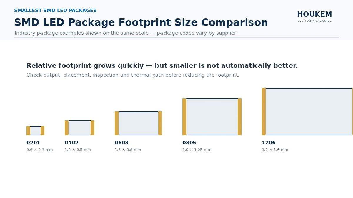
The four-digit codes used across the industry describe the nominal footprint of the part, not its height, its emitter area or its thermal capability. That is why two parts with the same code can differ in output, in viewing angle and in how much heat they can shed. To judge how small can an smd led be for a particular design, the footprint code is only the first of several figures that matter.
An smd led package size chart is useful for orientation, but it should be read together with the electrical and thermal ratings for the specific part. A package that is small enough mechanically can still be unusable if its thermal path cannot support the required drive level.
Why the Smallest Package Is Rarely the Answer
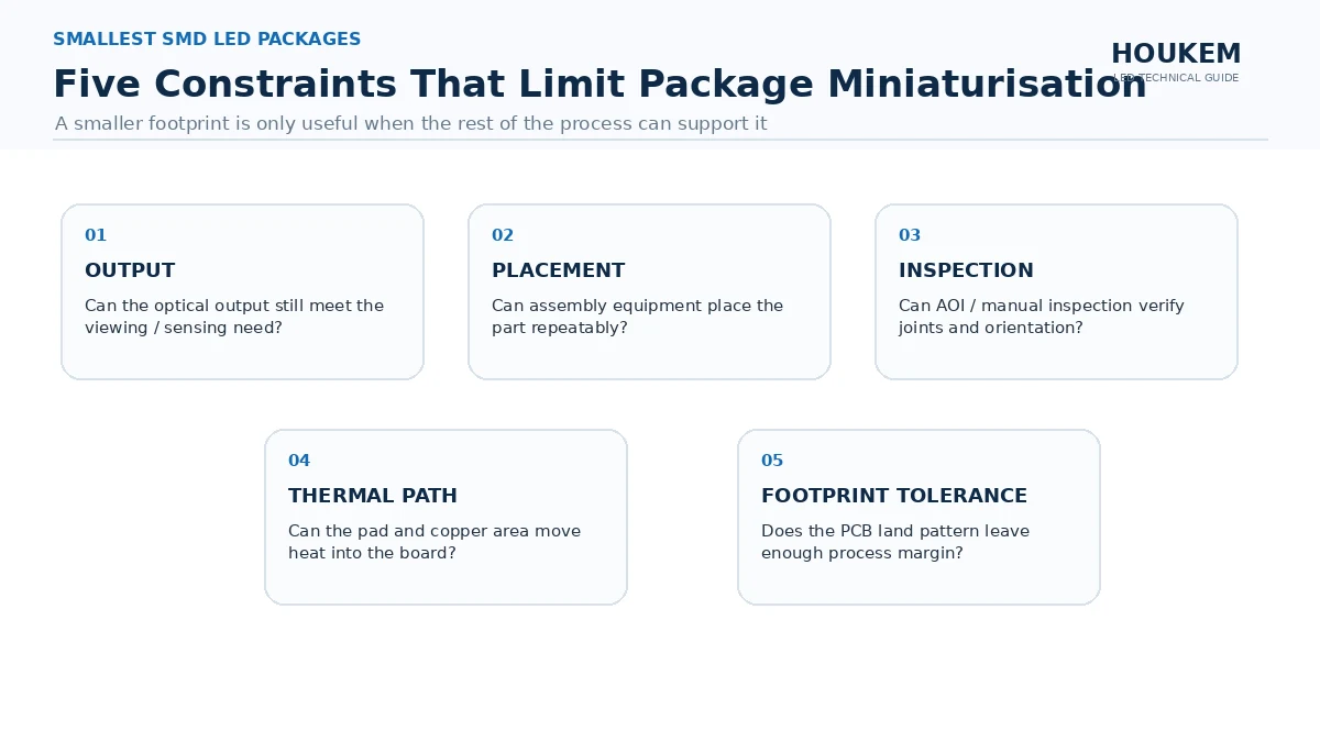
A smaller package normally carries a smaller emitter area, which reduces achievable output for the same drive current. It also carries less material to move heat away from the junction. Both effects push the design in the same direction, so the smallest available part often forces either a lower output target or a more elaborate thermal path than a slightly larger part would have needed.
| Constraint | What it limits | What to check before shrinking further |
|---|---|---|
| Required light output | Emitting area available in the package | Whether the brightness grade needed exists in the smaller package |
| Placement accuracy | The smallest pad pitch the line can place reliably | Placement tolerance and feeder capability on the actual machine |
| Inspection and rework | Whether joints can be seen and corrected | Optical inspection resolution and rework tooling |
| Thermal path | How much heat can leave through the joint area | Copper area and interface to the rest of the board |
| Footprint tolerance | How precisely the stencil and pad can be held | Stencil capability and solder volume control |
Placement, Inspection and Rework
When a package shrinks, the pad geometry shrinks with it, and the assembly process has to hold a tighter tolerance at every step. Placement accuracy, solder volume and the resolution needed to see the joint all move in the demanding direction at the same time. Once the process reaches its limit, further miniaturisation does not reduce risk; it transfers risk from the product to the production line.
Inspection is often the first capability to fail, because a joint that is acceptable in function may still be impossible to verify at production speed. Rework follows, since a part that cannot be inspected reliably is also a part that cannot be corrected cheaply. For compact industrial equipment the trade-off between a smaller part and a serviceable one is a real design decision, and it is discussed from the display side in miniature 7 segment displays in industrial equipment.
Thermal and Optical Limits
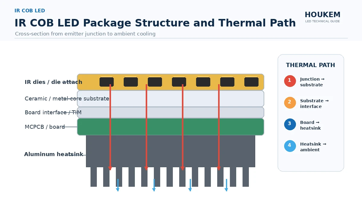
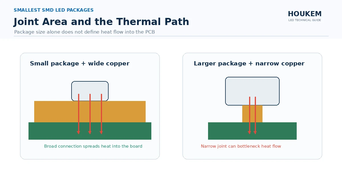
Thermal behaviour is where package size has the largest hidden effect, because the joint area is part of the thermal path. A small package with a large copper connection can outperform a larger package with a thin one, which is why led package size selection has to be evaluated against the board rather than in isolation. Where the board cannot take the heat away, the drive current must be reduced, and that reduction can cancel out the benefit of the smaller footprint.
Optically, a smaller emitter also changes the source size, which affects how a lens or light pipe can be used. If the design depends on a specific beam or on even illumination, the source area has to be checked before the package is reduced, because a smaller source is not automatically equivalent. Reading the relevant parameters correctly is the same discipline described in reading LED package specifications.
A Selection Sequence That Avoids Rework
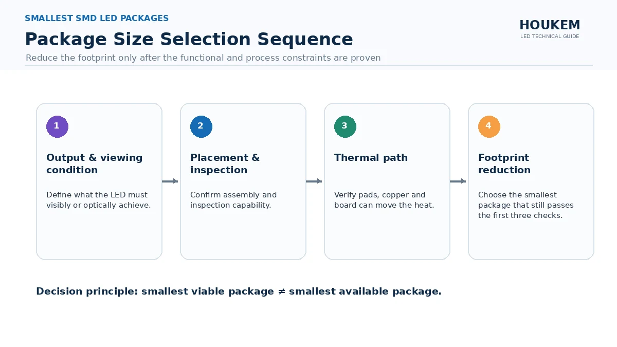
The constraints are easiest to handle in a fixed order. Start from the required light output and the viewing condition, then confirm that the placement and inspection capability on the actual line can hold the smaller footprint, then confirm that the thermal path through the board is sufficient at the intended drive current. Only when all three checks pass should the smd led footprint actually be reduced.
Where the design is a display rather than a single indicator, the size decision is driven by the viewing condition instead of by board area, and the relationship between size and readability is covered in matching display size to viewing distance. For compact numeric displays the practical options are covered by the SMD 7 segment display range, where digit height, not the four-digit package code, is usually the controlling dimension.
Confirming the Package Before Footprint Sign-Off
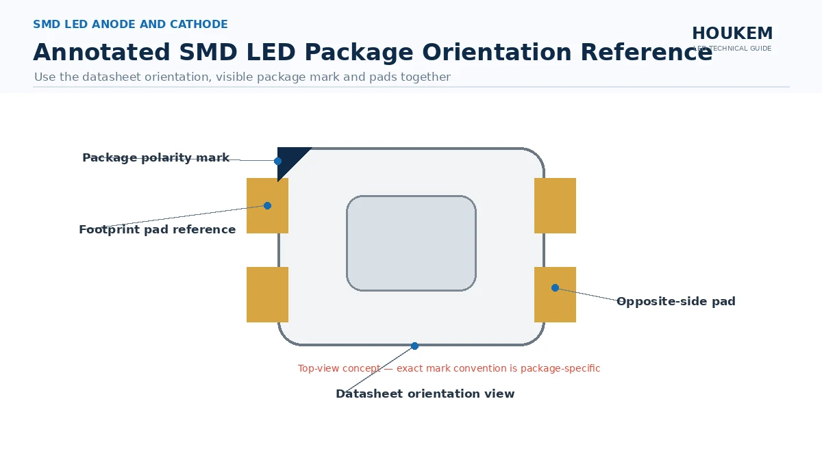
Before the footprint is released, the exact package code, the pad dimensions, the polarity orientation and the recommended solder profile should be confirmed for the specific part. It is also worth confirming that the required brightness grade is available in that package, because the smallest packages frequently offer a narrower range of output options than the mid-size ones, which can quietly force a redesign later.
Frequently Asked Questions
What is the smallest SMD LED package available?
Package naming follows an industry convention in which a four-digit code describes the nominal footprint, and the smallest codes in common use are well under one millimetre on a side. Availability for a specific part depends on the supplier and the required output, so the smallest available size must be confirmed per part.
Is the smallest package always the best choice?
No, because a smaller package usually carries less emitter area and less thermal mass. If the design needs light output or long-term stability, a slightly larger package often solves the problem with less risk.
What breaks first when a package gets too small?
Assembly tolerance usually becomes the limit before the component itself does, because placement accuracy, solder volume and inspection capability all tighten. Once those limits are reached, shrinking the package further moves risk into the production line rather than improving the product.
How does package size affect thermal behaviour?
A smaller package has less area to move heat into the board, so the thermal path has to be designed rather than assumed. Where the board cannot take that heat, the drive current has to be reduced, which removes the benefit of the smaller footprint.
How should package size be chosen for a compact product?
Start from the required light output and viewing condition, then check placement and inspection capability, then check the thermal path. Only if all three allow a smaller package should the footprint be reduced.
What should be confirmed with a supplier before finalising the footprint?
Confirm the exact package code, the pad dimensions, the polarity orientation and the recommended solder profile for the part. Also confirm that the output grade needed for the design is available in that package, because small packages often have fewer brightness options.
Choosing the Package Size Your Line Can Support
Shrinking an SMD LED package is a trade rather than a free gain. Each step down reduces the footprint, but it also reduces emitter area and thermal mass, and it tightens every tolerance in the assembly process. Designers who treat the four-digit package code as the only input usually rediscover that trade in production, when the footprint can no longer be changed cheaply.
Finding the smallest led package for compact pcb design is therefore a sequence rather than a search. If you describe the required output, the board area available and the assembly capability of your line, the applicable package options can be narrowed down, so describe your compact design envelope and include the constraint that is hardest to change.
SMD LED Anode and Cathode: How to Identify Polarity Correctly