


UV LED Array Spacing and Beam Overlap: Designing a More Uniform Exposure Area

Why Array Spacing Decides Exposure Uniformity
Each emitter in an array projects its own intensity cone onto the substrate, and the delivered pattern is the sum of all cones. Under the center of every emitter the irradiance peaks; between emitters it dips, and the depth of that dip depends almost entirely on how much the neighboring footprints overlap. When the peaks overlap strongly the surface reads as one even field, and when they barely touch the array prints its own layout onto the coating. This is the design-side counterpart of uniformity measurement, where a mapped grid reveals exactly these hot spots; the irradiance uniformity mapping guide covers how to measure the result. Spacing decides the problem before any instrument sees it, which is why it belongs in the design phase rather than the commissioning phase.
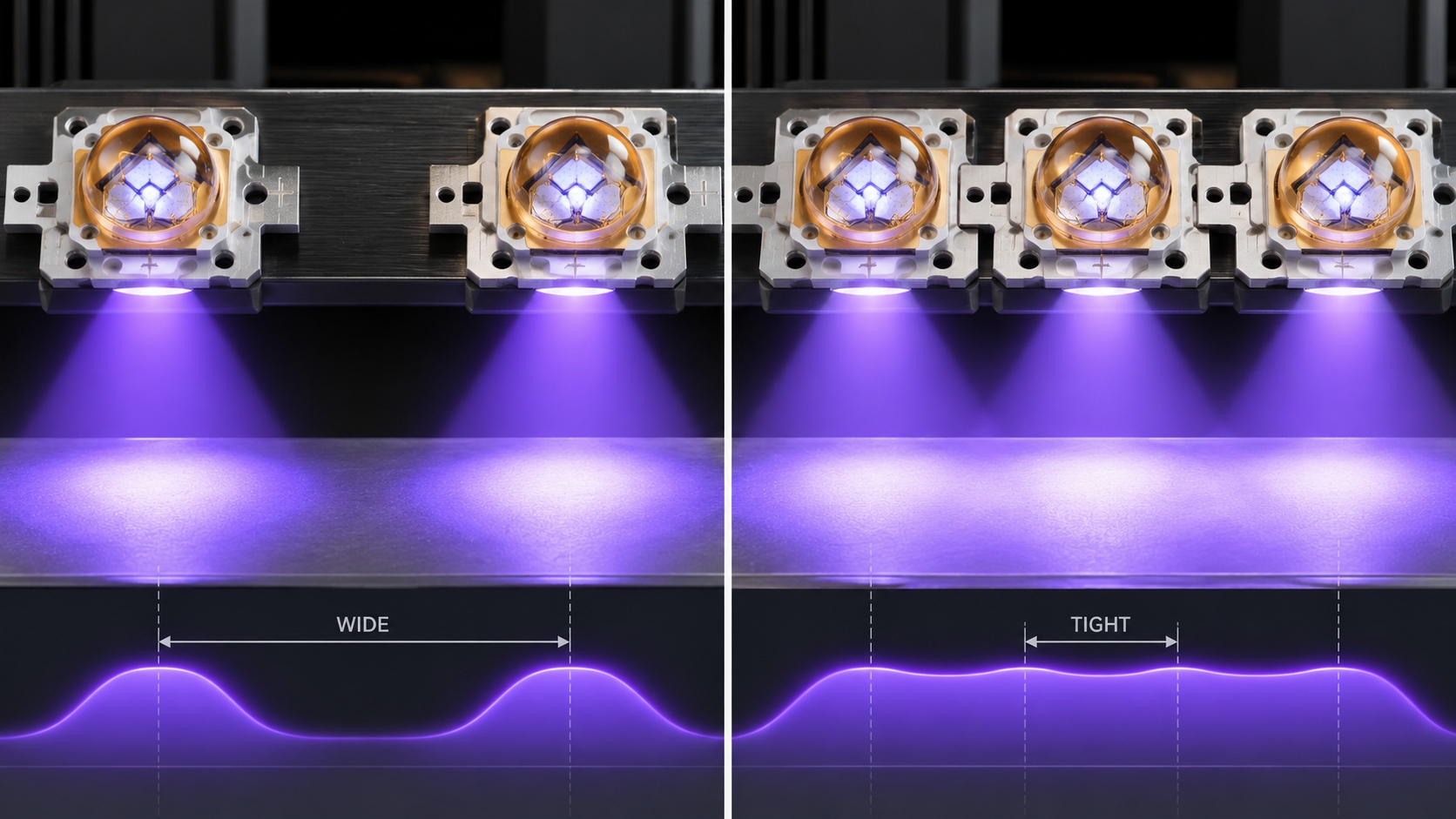
How Beam Overlap Changes the Uniformity of a UV LED Array
How beam overlap changes the uniformity of a UV LED array follows from three quantities: the beam angle of each emitter, the working distance, and the pitch between emitter centers. A wider beam angle or a larger distance produces a wider footprint at the substrate, so the same pitch yields deeper overlap. A tighter footprint at the same pitch leaves valleys. Edge falloff adds a second effect, because emitters at the array border have neighbors on one side only, so the outer rows always dip unless the array is oversized relative to the target area or a reflective window returns some of the border light. Secondary optics change the picture again, since a lensed emitter can hold a shaped footprint that bare chips cannot, and reflector geometry returns part of the spread. None of these effects can be read off a datasheet alone, because they combine at the substrate plane.
How to Plan UV LED Array Spacing for a Uniform Exposure Area
How to plan UV LED array spacing for a uniform exposure area starts from the requirement, not from the PCB outline. Define the exposure area the process needs, the minimum irradiance anywhere inside it, and the uniformity tolerance the coating or adhesive can accept. Then let the geometry set the pitch: estimate the footprint diameter from beam angle and working distance, choose a pitch that gives enough overlap to stay inside the tolerance, and oversize the array so border rows extend past the target. The table below summarizes the inputs and what each one pushes the design toward.
| Design Input | Where It Comes From | Effect on the Spacing Decision |
|---|---|---|
| Beam angle and optics | Emitter type, lens, reflector, protective window | Sets the footprint width that pitch must overlap |
| Working distance | Mechanical envelope, part clearance, thermal needs | Widens or narrows the footprint, changing the allowable pitch |
| Uniformity tolerance | Formulation sensitivity, process specification | Tighter tolerance forces tighter pitch or deeper overlap |
| Required irradiance | Line speed, target dose, formulation | Bounds how far the power can be spread across the area |
| Thermal budget | Emitter power, substrate material, cooling design | Tighter packing raises density and moves the thermal question forward |
The distance side of this trade-off deserves its own treatment, because the head height changes the footprint and therefore the whole pitch calculation; the UV LED working distance guide covers that interaction.
How Does UV LED Array Spacing Affect LED Performance
How does UV LED array spacing affect LED performance beyond the pattern on the substrate? Tighter packing raises the power density on the board, which raises the junction temperature of every emitter unless the thermal path grows with it, and output falls as the die warms. That is why spacing, drive current and cooling are one coupled decision in UV System Geometry & Optical Design rather than three separate line items. A sparse array with strong overlap from wide optics may deliver the same uniformity as a dense array of narrow-beam emitters while giving the heat far more room to leave. On high-power heads the coupling is direct, because the modules behind high-power 365nm UV LED systems need a thermal design that matches their electrical density; the high-power UV LED cooling guide treats that side in depth. Delivered energy over time remains the process target throughout, and the irradiance versus dose guide connects the spatial pattern to the dose the process actually needs.
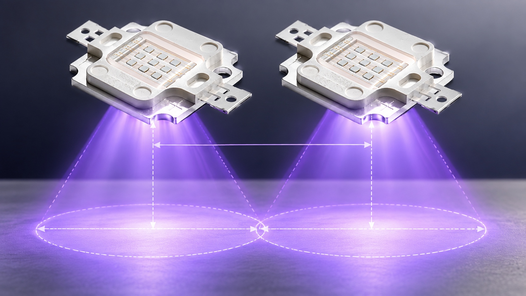
How Should Engineers Validate UV LED Array Spacing Before Production
How should engineers validate UV LED array spacing before production? With a measurement pass at the real substrate plane, not with a simulation alone. Map the exposure area on a grid with a calibrated radiometer matched to the wavelength band, at thermal steady state, and compare the peak-to-minimum ratio against the uniformity tolerance the process declared. Repeat the map after the head has warmed and after any optics or window cleaning, because small mechanical changes move the overlap. Record the map next to the head height and drive settings so the layout can be reproduced and audited later. If the valleys between emitters show up in the map, the fix is geometric, either tighter pitch or more overlap from optics, and changing it before tooling is far cheaper than chasing the same pattern through process tweaks in production.
Frequently Asked Questions
Does a denser array always give better uniformity?
Higher density deepens the overlap between footprints, which usually flattens the field between emitters. It also raises thermal density and cost, so the right pitch is the one that meets the uniformity tolerance with margin, not the tightest one that fits.
Can reflectors or windows replace proper spacing?
Reflective surfaces and diffusing windows soften valleys and help the border rows, which makes them useful allies. They redistribute light rather than create it, so a layout that depends on them still needs a measured map to confirm the result.
Should spacing change when the working distance changes?
Yes, because the footprint grows with distance and the same pitch produces deeper overlap at a greater height. A layout tuned at one height can fall out of tolerance when the head is raised or lowered without recalculating the overlap.
How is uniformity expressed in a specification?
Most process specifications state a minimum and maximum irradiance across the defined exposure area, and uniformity is the ratio between them. Writing the requirement that way gives the array designer a number to design against instead of a vague request for even coverage.
Is the same spacing right for different wavelengths?
The geometry of overlap depends on optics and distance rather than on wavelength, so the pattern logic is the same. The formulation responds differently to each band, however, so the irradiance the layout delivers still has to match the wavelength-specific process requirement.
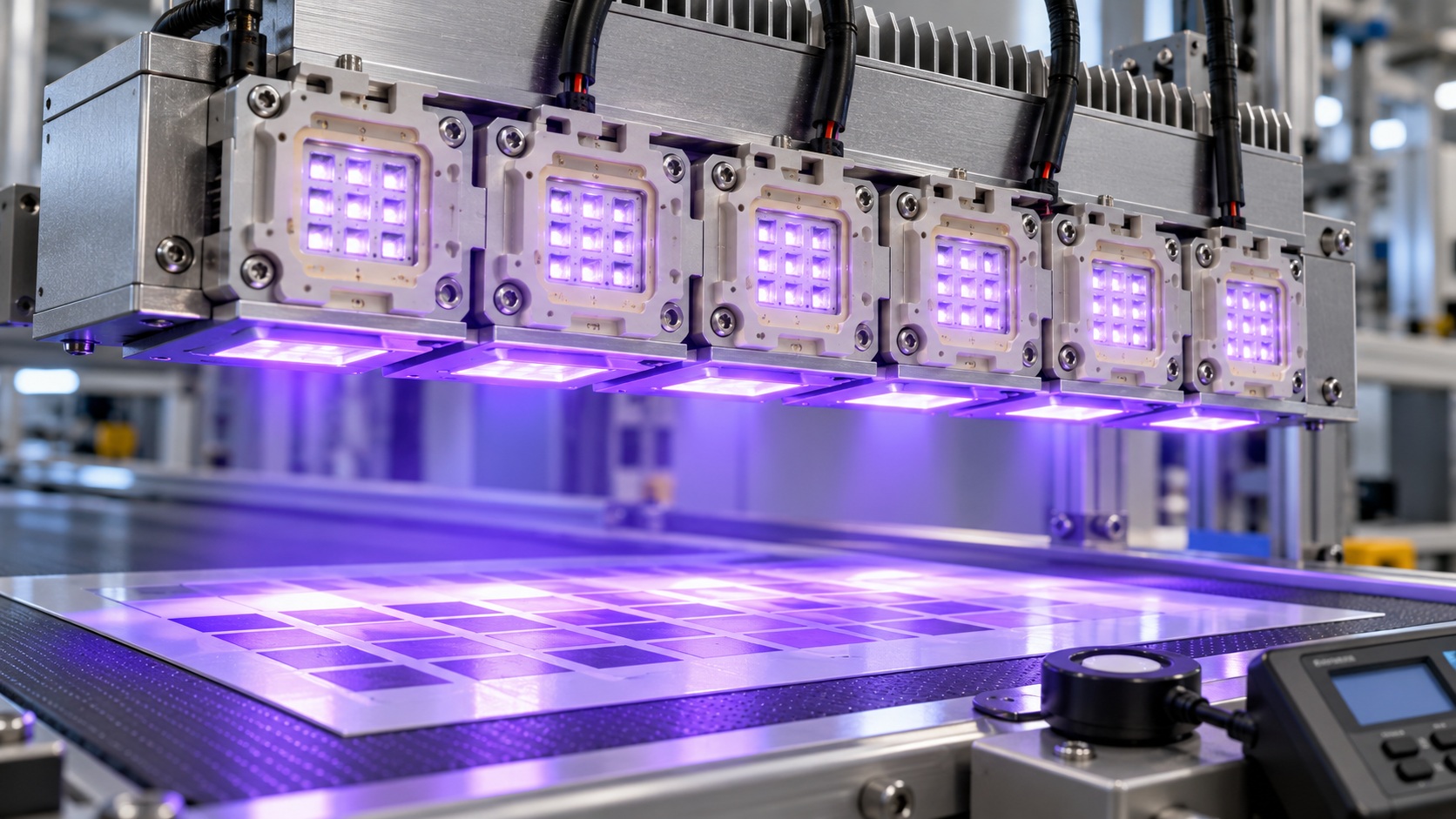
Bringing the Array Design Together
A uniform exposure area is designed, not discovered: beam angle, working distance and UV LED array spacing set the overlap, the thermal budget sets its limits, and one mapped measurement pass confirms all three before production. Handled in that order, UV LED array spacing becomes a documented design parameter instead of a pattern that shows up later in the cure results. If you are engineering a UV LED curing or exposure system and want the array geometry reviewed against your uniformity target, send your layout requirements to HOUKEM and the engineering team will support the design-in.
UV LED Irradiance Uniformity: How to Map Hot Spots Across the Curing Area


