LED Solder Joint Thermal Cycling: How Cyclic Stress Fatigues Joints
Quick Answer: CTE Mismatch Turns Temperature into Strain
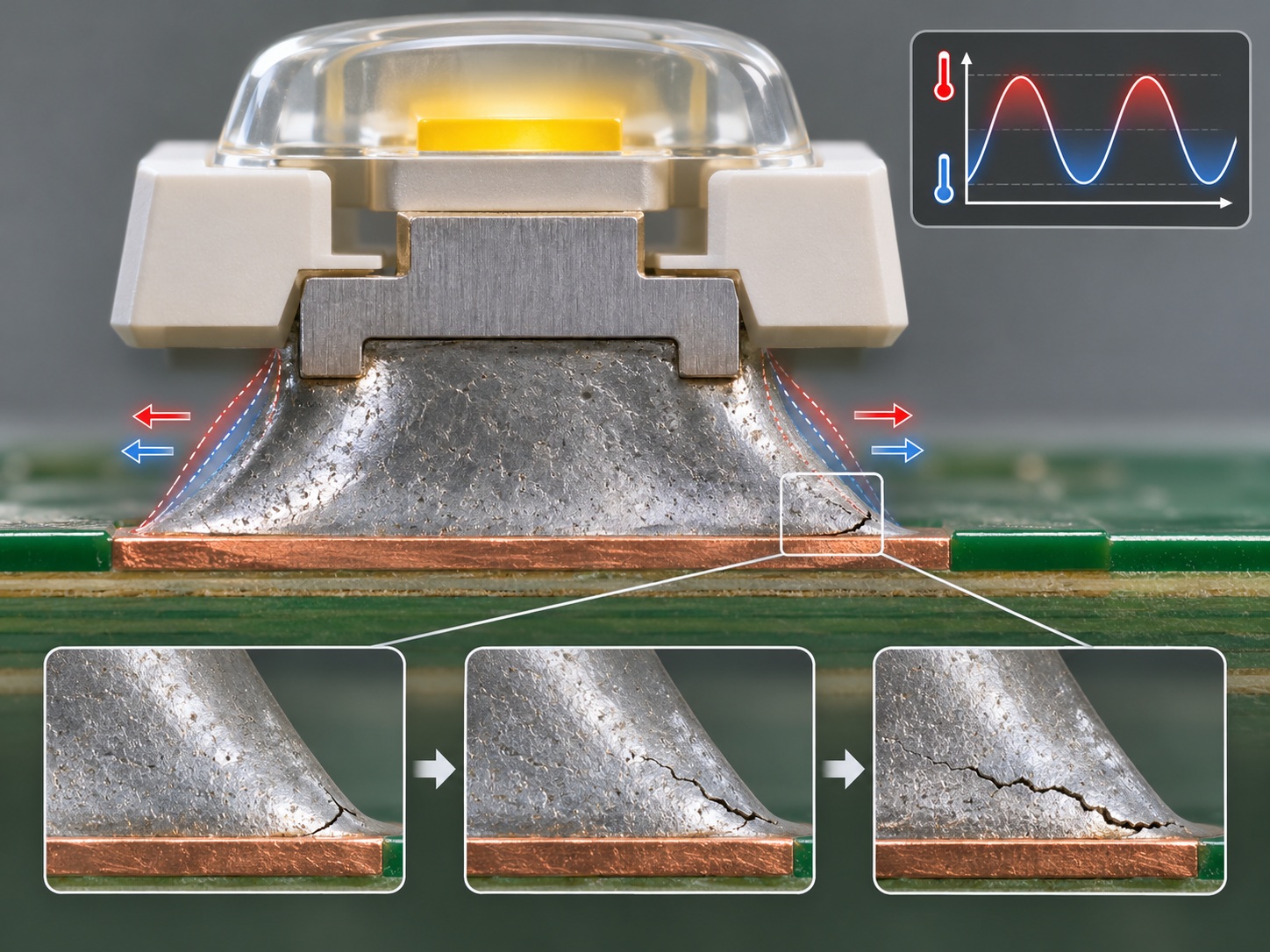
Silicon, copper, FR4 and ceramics each expand at their own rate as temperature changes. When these materials are joined by a solder layer, the differences force the joint to shear slightly on every cycle. One excursion does nothing visible. Thousands of excursions accumulate creep damage in the solder, and eventually a crack propagates through the joint. This is LED solder fatigue, and it explains why failures cluster in products with wide temperature swings, large packages and rigid connections.
The Thermal-Cycle Mechanism Step by Step
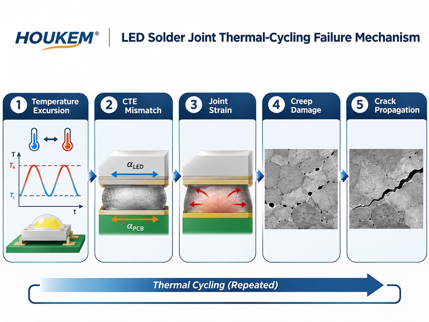
The sequence of how thermal cycling damages LED solder joints is worth understanding in order, because each step suggests a different control:
- The assembly heats and cools with power cycling, ambient changes or sunlight load.
- Each material in the stack expands according to its own coefficient of thermal expansion.
- Because the materials are bonded, the mismatch is absorbed as strain in the solder and in the package leads.
- Repeated strain produces creep deformation, then micro-cracks, typically starting at the joint edge where stress concentrates.
- The crack grows across the joint until resistance rises or the connection opens intermittently.
The intermittent stage is the treacherous one. A joint that opens only when cold or only when flexed passes bench testing and fails in the field, which is why a pattern of LED solder joint failure thermal cycling produces often looks random until the temperature correlation is noticed.
Which Design Factors Set the Risk
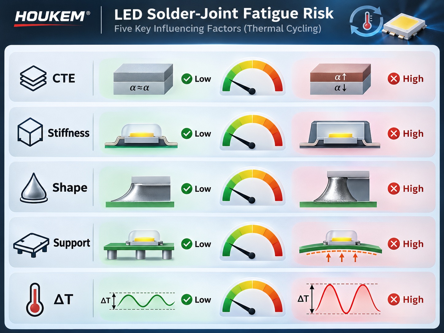
Not every assembly carries the same exposure. The risk is set by geometry and materials long before the first cycle runs:
| Factor | Lower Risk | Higher Risk |
|---|---|---|
| CTE spread across the stack | Matched materials, such as MCPCB under high-power parts | Large mismatch, such as ceramic die on FR4 without underfill |
| Package size and stiffness | Small compliant packages with flexible leads | Large rigid packages with heavy solder volumes |
| Solder volume and shape | Full, convex fillets with controlled thickness | Starved joints or excessive, stiff solder mass |
| Board support | Display load carried by stand-offs, not the joints | Joints acting as structural elements |
| Temperature swing amplitude | Narrow, slow cycles near room temperature | Wide, fast cycles from outdoor or power switching loads |
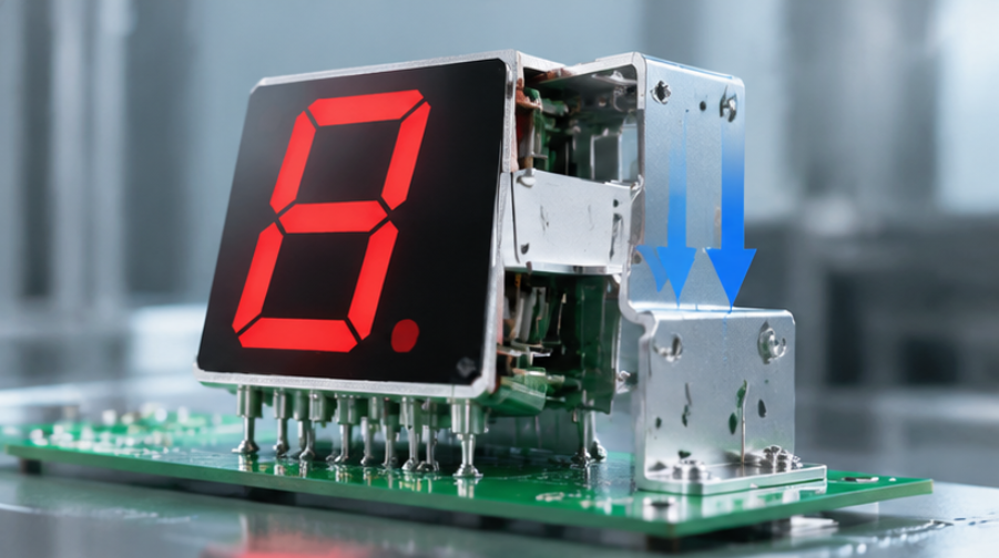
Substrate choice is the single most leveraged decision, which is why our comparison of MCPCB and FR4 for LED thermal design treats mechanical fit alongside thermal performance. For display products, mechanical load management is equally decisive: the guide to mounting large 7-segment displays insists that the solder joint never serve as a structural element, a principle that removes the largest single stress contribution in one design step.
Assembly Quality Interacts with Design Risk
A sound design can still be undermined by assembly. Voided joints, starved fillets and misaligned parts all concentrate strain into less solder area, so the same thermal cycling LED PCB design yields different fatigue lives depending on process control. The reflow profile determines the microstructure and void content of the joint, and our guide to reading LED reflow profiles explains which zones to verify. Dimensional variation matters too: coplanarity and stack-up tolerances decide whether every joint carries an equal share of the strain, which the analysis of LED display PCB assembly tolerances covers in detail. Where joints are suspect, X-ray sampling on the critical packages during a controlled inspection finds voids before they become field failures. A void or a starved fillet is a ready-made LED solder crack initiation site, which is why process capability belongs next to design margin in the risk review.
Validating Against Thermal Cycling
Validation converts the design intent into evidence. Temperature cycling tests exercise assemblies between defined extremes for a set number of cycles, with electrical monitoring to catch the intermittent opens that visual inspection misses. The test parameters that matter most are the temperature extremes, the ramp rate, the dwell time and the number of cycles, and they should resemble the product's real environment rather than a generic standard. Complement cycling with cross-section analysis on sampled joints, which shows crack initiation sites and void content directly. For the thermal side of the same assembly, our guide on thermal resistance quantifies the steady-state conditions that the cycles are superimposed on.
Frequently Asked Questions
How thermal cycling damages LED solder joints over time?
Each temperature swing forces materials with different expansion rates to shear the solder slightly. The repeated strain accumulates as creep damage, micro-cracks form at the joint edge, and a crack eventually grows until the connection opens or turns intermittent.
Why do solder joint failures appear intermittent at first?
A partially cracked joint still conducts when warm and closed, but opens when cold or flexed. The symptom follows temperature or vibration, which distinguishes fatigue from a permanent open circuit.
Does a bigger solder joint always last longer?
No, because excessive stiff solder transmits more strain to the joint instead of absorbing it. A controlled, compliant joint shape with a proper fillet outperforms a heavy mass of solder.
Can underfill or compliant adhesives reduce the risk?
Yes, when they are designed in, because they distribute strain away from the solder layer. They add process complexity, so the decision belongs in the design phase with supplier input rather than as a field retrofit.
Is LED PCB solder fatigue visible at incoming inspection?
Fatigue cracks are not visible before they form, but their preconditions often are: voids, starved fillets and misalignment show up in X-ray and optical checks. Catching those preconditions is the practical inspection strategy.
Which products need thermal cycling validation most?
Products with wide ambient ranges, frequent power switching, large display formats or stiff package connections carry the highest exposure. Automotive, outdoor and industrial control applications belong at the top of the list.

Conclusion: Design the Strain Out Before the Cycles Begin
LED solder joint thermal cycling failure is cumulative, predictable and largely designed-in. Match materials where you can, let stand-offs carry the loads, control the assembly quality that concentrates strain, and validate with cycling that resembles the real environment. If you are selecting LED packages and substrates for a high-cycle application, our engineering team can discuss package construction and mounting options through the inquiry page.